annular-width
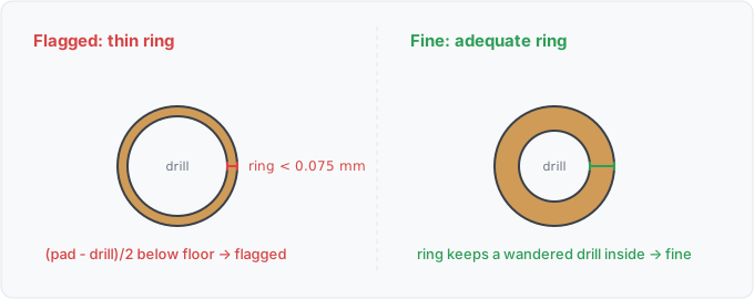
A via's annular ring is thinner than the minimum the board declares, or the loosest common fabrication floor (0.075mm) when it declares none.
Remedy 
Enlarge the pad or reduce the drill until the annular ring clears the fab’s floor with tolerance left over for drill wander.
What it means 
A via’s copper ring, (pad diameter minus drill) / 2, is below the board’s declared minimum annular width. When the board declares none, the limit is 0.075mm, the loosest mainstream floor (the corpus JLCPCB rules).
Why engineers want it 
Drills wander within tolerance; the annular ring is the margin that keeps a wandered drill inside its pad. Too little ring means breakout, where the barrel sits tangent to (or outside) the pad edge.
Impact 
Intermittent or open via connections that pass visual inspection.
Scope note 
Same floor-default posture as track-width. A board that declares its own minimum is held to that instead, because the declaration is the designer saying which process the board is routed for. Today the only such declaration is a KiCad project’s board.design_settings.rules, read whichever of the project’s files names the design. Every finding names which of the two limits it was measured against (agni issue 933).
Query structure 
select nets with any via whose ring is below the floor.
select N in board.nets where count(V in N.vias where annular(V) < floor) >= 1
where floor is the declared minimum via annular width, else 0.075mm.
Reads: board.copper, board.rules. Tier P.