copper-clearance
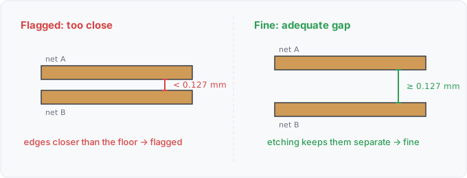
Copper of two different nets sits closer than the 0.127mm fabrication floor.
Remedy 
Pull the two nets apart to the fab’s minimum clearance. A gap below it is a short waiting on etch variance or a solder bridge.
What it means 
Two track segments on the same copper layer, belonging to different nets, whose copper edges (centerline distance minus half of each width) come closer than 0.127mm (5mil), the loosest mainstream fab’s minimum spacing (the corpus JLCPCB rules).
Why engineers want it 
Clearance is the other half of every fab capability sheet. Below it, etching cannot guarantee separation and solder bridges what etching spared: the board acquires connections the schematic never had.
Impact 
Order-time rejection at best; intermittent shorts in the field at worst.
Scope note 
Segment-to-segment on the same layer only: pad and zone clearances wait on pad-shape geometry facts, and same-net spacing is not a defect. The pairwise walk is O(S²) with an early bounding-box reject; fine at corpus scale (hundreds of segments), and the benchmark documents where a spatial index (WS3-004) becomes necessary. One finding per net PAIR, subject = the alphabetically first net, message naming both and the worst gap.
Query structure 
the pairwise spatial join the Phase-1 AST does not express:
select (S1, S2) in board.segments x board.segments
  where net(S1) != net(S2) and layer(S1) == layer(S2)
    and edge_distance(S1, S2) < 0.127mm
Reads: board.copper. Tier P. Primitives: select, geometry-distance (candidate primitive, not yet in the AST, and this rule is its evidence).