track-width
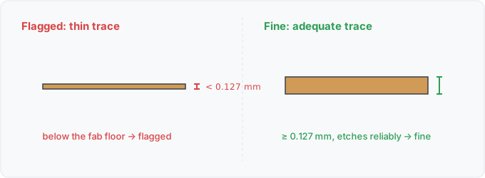
A routed track is narrower than the loosest common fabrication floor (0.127mm).
Remedy 
Widen the track to the fab’s minimum, or move the board to a process quoted for the width you need. Below the floor a trace will not etch reliably at mainstream yields.
What it means 
A routed copper segment narrower than 0.127mm (5mil), the minimum trace width of the loosest mainstream fabrication capability (the corpus JLCPCB rule set).
Why engineers want it 
Track width is the first constraint every fab publishes and every DRC ships. A sub-minimum trace is not a style choice: the fab rejects the board or etches it unreliably.
Impact 
Order-time rejection at best; intermittent opens and current failures at worst.
Scope note 
The 0.127mm default is deliberately the loosest published floor, so the rule fires on defects rather than on deliberate tight routing under a capable fab’s own rules; per-design thresholds arrive with rule parameterization (WS3-006). Available gates the rule behind the board-geometry tier (a netlist-only design reports “unavailable”, not a silent pass).
Query structure 
select nets with any segment below the floor.
select N in board.nets where count(S in N.segments where width(S) < 0.127mm) >= 1
Reads: board.copper. Tier P.